ANALYSIS TYPE / 01
Pixel-Level Response · QE · Optical Crosstalk
Overview
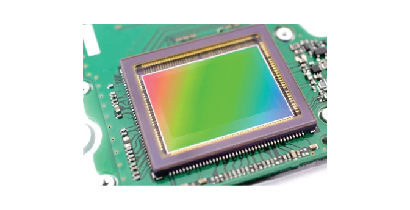
CMOS image sensor simulation models the optical response of pixel arrays, microlens efficiency, angular sensitivity, cross-talk, and quantum efficiency — enabling optimised sensor architecture for automotive, smartphone, and industrial imaging applications. Accurate photon transport simulation through the full optical stack — from microlens array through colour filter array and passivation to the photodiode — predicts the spectral QE, CRA response, and MTF degradation from crosstalk before any silicon mask tape-out.
Industries Served
Deliverables
Key Aspects
Simulating the focusing efficiency of microlens arrays over each pixel — optimising lens shape, pitch, and material to maximise light collection and reduce optical crosstalk.
Computing spectral quantum efficiency by tracing photons through the optical stack into the photodiode — guiding passivation, AR coating, and deep trench isolation design.
Evaluating the sensitivity drop at high chief ray angles (CRA) across the full image field — matching the sensor CRA characteristic to the camera lens design.
Quantifying optical crosstalk between adjacent pixels and its impact on the modulation transfer function — guiding deep trench isolation geometry and colour filter design.
Connect with our optics & photonics simulation team to discuss the right approach for your application.