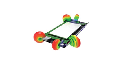
PDN · decoupling strategy · voltage noise · DC IR drop
Power delivery network analysis ensuring stable, low-noise supply voltage to all ICs — from target impedance definition and decoupling optimisation through voltage droop, SSO noise, and package co-simulation across the full operating frequency range.
What We Deliver
Power integrity failures manifest as system resets, data corruption, and functional failures that are difficult to diagnose in hardware. Our power integrity team analyses the full power delivery path — from voltage regulator through PCB planes and package to IC silicon — identifying impedance peaks, voltage droop, and current hotspots before prototype builds.
We cover PDN impedance analysis, decoupling capacitor optimisation, voltage droop and SSO noise, power plane resonance, DC IR drop, and package PDN co-simulation across all IC power domains on your board.
Key Problems We Solve
6 Analysis Areas
Select a capability to explore the methodology, deliverables, and tools in detail.
ANALYSIS TYPE / 01
target impedance · frequency response · Z-profile
Characterising power delivery network impedance across the full frequency range — from DC through multi-GHz — to ensure the impedance profile remains below the target impedance budget for all IC power domains on the board.
Key Aspects
Computing the maximum allowable PDN impedance for each power rail based on IC load current transients, supply voltage tolerance, and acceptable ripple budgets.
Simulating PDN impedance versus frequency including VRM, bulk capacitors, ceramic bypass capacitors, and PCB plane inductance — identifying resonant peaks that exceed targets.
Analysing multiple power domains simultaneously to identify coupling between adjacent power planes and shared return paths that degrade power integrity performance.
Correlating simulated PDN impedance with physical VNA measurements for model validation and iterative design improvement before final board release.
ANALYSIS TYPE / 02
capacitor selection · placement · anti-resonance
Optimising decoupling capacitor selection, value, quantity, and placement to flatten the PDN impedance profile — avoiding anti-resonance peaks while achieving the minimum capacitor count and cost for each power domain.
Key Aspects
Selecting optimal capacitance values and ESR/ESL profiles to fill specific frequency bands in the impedance profile, minimising total component count without sacrificing performance.
Determining capacitor placement relative to IC power pins, via positions, and reference planes to minimise loop inductance and maximise decoupling effectiveness at operating frequencies.
Identifying and resolving anti-resonance peaks between bulk and ceramic capacitor stages that cause localised impedance spikes exceeding target impedance at specific frequencies.
Iterating the decoupling strategy to achieve specification compliance with the fewest, lowest-cost capacitors — balancing SI performance against PCB area and bill of materials budget.
ANALYSIS TYPE / 03
transient response · simultaneous switching · noise budget
Analysing voltage droop and simultaneous switching output noise to ensure all IC power pins remain within datasheet supply tolerance during worst-case switching events — validating timing margin and functional reliability.
Key Aspects
Simulating power supply voltage droop during IC load current step events, computing worst-case undershoot and recovery time relative to datasheet supply tolerance limits.
Evaluating voltage noise induced on power and ground planes by simultaneous switching of multiple output drivers — identifying timing margin risk in high-driver-count interfaces.
Computing ground bounce magnitude at IC VSS pins during large current transients, assessing impact on internal logic switching thresholds and setup/hold timing.
Partitioning the total power supply noise budget across PDN, decoupling, and plane inductance contributors to guide prioritised design improvements.
ANALYSIS TYPE / 04
cavity resonance · plane modes · standing waves
Identifying power and ground plane cavity resonances that cause high-impedance peaks in the PDN at specific frequencies — analysing standing wave patterns and recommending anti-pad geometry, plane splits, or additional damping to suppress resonances.
Key Aspects
Computing resonant modes of power and ground plane pairs as parallel-plate resonant structures, identifying frequencies where the PDN exhibits high-impedance resonant behaviour.
Mapping the spatial distribution of resonant mode standing waves across the PCB surface to identify high-noise-sensitivity regions for critical IC placement.
Evaluating how anti-pads, cutouts, and plane splits modify cavity resonance frequencies and Q-factors, and assessing their PDN impedance impact.
Recommending embedded capacitors, EBG structures, or ferrite material strategies to damp cavity resonances without significantly increasing PDN impedance at lower frequencies.
ANALYSIS TYPE / 05
current density · voltage drop · thermal hotspots
Performing DC analysis of power distribution networks to identify current crowding, excessive IR drop, and copper trace thermal hotspots — ensuring all power pins receive sufficient voltage and no trace segment exceeds thermal design limits.
Key Aspects
Mapping DC current distribution across power and ground planes to identify current crowding regions where copper resistance causes voltage drop and localised heating.
Evaluating current sharing across via arrays and identifying under-designed via connections that carry excessive current density relative to IPC-2152 current capacity guidelines.
Predicting Joule heating in high-current conductors to identify copper features approaching thermal limits and guide trace width or via count corrections.
Generating spatial voltage maps across all power rails to confirm that worst-case receiving IC power pins remain within datasheet minimum supply voltage specifications.
ANALYSIS TYPE / 06
IC package · board PDN · co-optimisation
Co-simulating IC package and board PDN together to capture the interaction between on-package capacitance, package plane inductance, and board-level decoupling — providing a complete system-level power integrity assessment.
Key Aspects
Incorporating vendor-provided IC package S-parameter or SPICE models into the board-level PDN simulation to capture the complete power delivery path from VRM to silicon.
Evaluating the contribution of on-package decoupling capacitors to board-level PDN impedance, determining how much additional board decoupling is required versus package-integrated capacitance.
Identifying resonances introduced by the interaction between package and board PDN structures — particularly the inductance of the package-to-board interface vias and balls.
Optimising the combined package and board decoupling strategy as a unified system, minimising total capacitor count and cost while meeting package-level and board-level impedance targets.
Talk to our Centre of Excellence team about PDN impedance, decoupling strategy, voltage droop, or DC IR drop analysis for your board design.