Pre-compliance · radiated emissions · conducted noise · shielding · immunity
Electromagnetic compatibility simulation for pre-compliance verification — predicting radiated and conducted emissions, shielding effectiveness, susceptibility, cable coupling, and PCB layout EMC risk before the first chamber test.
What We Deliver
EMC chamber failures late in the development cycle are among the most expensive compliance issues to resolve — requiring hardware spins, re-testing cycles, and delayed market entry. Our EMC simulation team identifies emission sources, susceptibility paths, and shielding deficiencies in the design phase, when corrections are inexpensive and rapid.
We cover radiated and conducted emissions, shielding effectiveness, susceptibility and immunity, cable and harness coupling, and PCB layout optimisation — providing actionable pre-compliance reports mapped directly to CISPR, IEC 61000, ISO 11452, and automotive EMC standards.
Key Problems We Solve
6 Analysis Areas
Select a capability to explore the methodology, deliverables, and tools in detail.
ANALYSIS TYPE / 01
pre-compliance · far-field · EMC chamber correlation
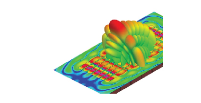
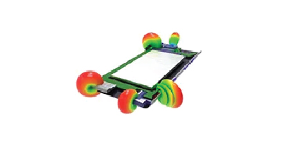
Predicting radiated emissions from PCBs, cables, and enclosures before the first EMC chamber test — identifying dominant emission sources, frequencies, and antenna structures that drive non-compliance and enabling targeted layout corrections.
Key Aspects
Computing far-field radiated emission profiles from PCB and system models, comparing predicted emissions against CISPR 22/32, FCC Part 15, and automotive CISPR 25 limits.
Tracing dominant emission sources to specific PCB structures — switching regulators, clock lines, high-speed interfaces — quantifying each contributor's share of the total radiated emission budget.
Performing near-field to far-field transformation from board-level field scans or simulation data, enabling correlation with physical chamber measurements.
Providing a structured pre-compliance risk report identifying emission peaks most likely to fail chamber testing and prioritising corrective actions by impact and implementation effort.
ANALYSIS TYPE / 02
LISN · power line noise · filter design
Simulating conducted emissions on power and signal lines — predicting noise voltage and current measured at LISN points and designing input filters to achieve compliance with CISPR 11/22/32 conducted limits.
Key Aspects
Modelling conducted emission measurement setups including LISN impedance, referencing simulated results to the standardised CISPR measurement methodology for direct limit comparison.
Separating conducted noise into common mode and differential mode components to determine the appropriate filter topology — X-capacitors, Y-capacitors, common mode chokes — for each noise mechanism.
Designing and optimising EMI input filters for switching power supplies and motor drives — selecting component values, insertion loss targets, and filter topology to achieve CISPR compliance.
Modelling conducted noise generated by DC-DC converters and analysing how PCB layout, transformer construction, and output filtering affect LISN-measured emission levels.
ANALYSIS TYPE / 03
enclosure · aperture analysis · gasket design
Analysing shielding effectiveness of electronic enclosures — evaluating aperture leakage from vents, seams, connectors, and display openings, and quantifying how structural shielding reduces both radiated emission and susceptibility to external fields.
Key Aspects
Computing electromagnetic leakage through enclosure apertures — cooling vents, cable entries, display cutouts, and seam gaps — identifying which openings dominate the shielding effectiveness degradation.
Identifying resonant cavity modes within the enclosure that amplify internal fields at specific frequencies, creating emission peaks or susceptibility hotspots on sensitive circuits inside.
Evaluating the effectiveness of conductive gaskets, finger stock, and paint treatments at enclosure seams and connector interfaces — computing required contact resistance and gasket compression for target shielding levels.
Analysing PCB-mounted shielding can effectiveness for isolating high-frequency circuits from adjacent sensitive areas within the same enclosure, including aperture effects for programming access holes.
ANALYSIS TYPE / 04
ESD · BCI · radiated immunity · IEC 61000
Evaluating electronic system immunity to conducted and radiated disturbances — simulating ESD events, bulk current injection, and radiated field exposure to predict susceptibility before IEC 61000, ISO 11452, and DO-160 chamber testing.
Key Aspects
Modelling IEC 61000-4-2 ESD contact and air discharge events, tracing current paths through the PCB to IC pins and evaluating the adequacy of TVS protection and layout shielding.
Simulating ISO 11452-4 BCI test setups to predict induced voltage and current levels at IC inputs from cable injection — validating filter and ferrite protection effectiveness.
Computing induced voltages on PCB traces and cable harnesses from external radiated fields per IEC 61000-4-3 and ISO 11452-2, identifying sensitive circuit nodes at risk of upset.
Documenting susceptibility margin above required test levels for each disturbance type, identifying circuits with marginal immunity and recommending targeted hardening measures.
ANALYSIS TYPE / 05
differential-to-common mode · shield transfer · crosstalk
Analysing electromagnetic coupling along cable harnesses and wire bundles — evaluating differential-to-common mode conversion, shield transfer impedance, inter-wire crosstalk, and cable radiation to address the most frequent source of system-level EMC failures.
Key Aspects
Identifying impedance imbalances, asymmetric loads, and connector transitions that convert differential signal content to common mode current — the primary source of cable radiated emissions.
Evaluating cable shield effectiveness using transfer impedance models, comparing braided, foil, and combination shields for their performance over frequency and at connector terminations.
Computing inter-wire crosstalk in multi-conductor harnesses for automotive and aerospace applications — evaluating signal-to-power, signal-to-signal, and control-to-power coupling across bundle cross-sections.
Modelling cable assemblies as unintentional antennas and predicting their radiated emission levels, identifying cable routing, length, and termination changes that reduce emission without physical re-routing.
ANALYSIS TYPE / 06
return current · split planes · routing for EMC
Reviewing and optimising PCB layout for EMC compliance — analysing return current paths, plane split crossings, high-frequency loop areas, and decoupling placement to reduce emissions and improve immunity at the board level.
Key Aspects
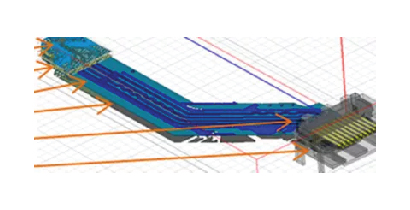
Mapping return current distribution under high-speed signal traces to identify where return paths are forced to detour through splits, anti-pads, or adjacent planes — creating emission-inducing loop areas.
Identifying large current loop areas formed by power and signal routing, and recommending trace routing, layer assignment, and decoupling placement changes to minimise loop area at critical frequencies.
Evaluating the EMC impact of plane splits, moats, and routing-across-cuts on high-speed interface traces, and recommending layout changes or stitching capacitors to maintain return current continuity.
Reviewing placement of oscillators, switching regulators, filters, and connectors relative to sensitive circuits and PCB boundary to minimise intra-board coupling and external radiation.
Talk to our Centre of Excellence team about radiated emissions, conducted noise, shielding design, or immunity analysis for your product development programme.