GaN and SiC Semiconductors: Pioneering the Future of Power Electronics
Wide-bandgap semiconductors such as GaN and SiC are reshaping electric vehicles, renewable energy, aerospace and consumer electronics — and Ansys simulation is catalyzing their real-world impact.
S
Sagarika
May 2, 20255 min read
1. Catalyzing the Next Era of Power Electronics
Imagine an electric vehicle that recharges in under 15 minutes, mirroring the convenience of conventional fueling or a palm-sized laptop adapter that remains cool even during intense workloads. These are no longer far-fetched dreams, but rapidly advancing realities, enabled by the disruptive capabilities of Gallium Nitride (GaN) and Silicon Carbide (SiC) semiconductors.
For decades, silicon has been the industry standard in power electronics. But as global demand escalates for compact, efficient, and high-speed systems, silicon is reaching the upper bounds of its performance envelope. In this context, wide-bandgap semiconductors such as GaN and SiC are emerging as pivotal technologies reshaping paradigms across electric vehicles, renewable energy infrastructure, aerospace, and high-performance consumer electronics.
What precisely makes these materials the cornerstone of next-generation power solutions? Let's delve into their scientific foundations, industrial applications, and how simulation platforms like Ansys are catalyzing their real-world impact.
2. The Ascent of Wide-Bandgap Semiconductors
Tracing the Evolution
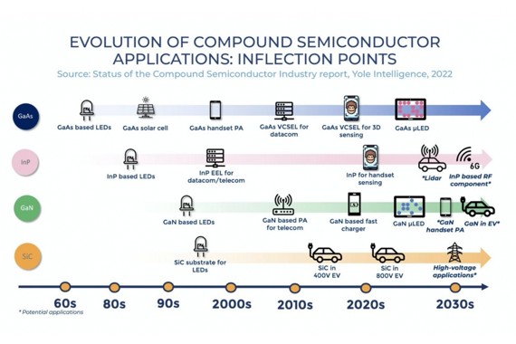
The story of GaN and SiC is interwoven with the broader evolution of power electronics — a field driven by the imperative to achieve higher voltage thresholds, enhanced thermal stability, and faster switching frequencies. While silicon laid the groundwork, its material constraints sparked the pursuit of alternatives.
Key Developmental Milestones:
1980s – SiC's remarkable thermal conductivity attracted early attention for high-power electronics.
1990s – GaN-based HEMTs (High Electron Mobility Transistors) demonstrated exceptional switching speed, ideal for RF and high-frequency applications.
2000s – SiC MOSFETs entered the commercial landscape, offering a leap in power conversion efficiency.
2020s – GaN dominates compact consumer electronics while SiC leads in EV traction inverters and industrial systems.
These milestones didn't just improve existing technologies — they enabled innovations once considered unfeasible.
3. Demystifying the Physics of GaN and SiC
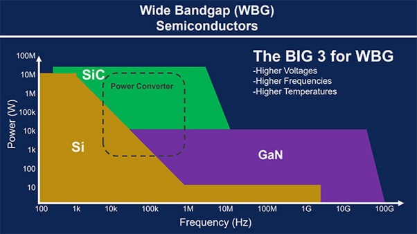
At the core of GaN and SiC's game-changing performance lies their wide bandgap structure. Unlike silicon, which has a bandgap of 1.1 eV, GaN (3.4 eV) and SiC (3.3 eV) can tolerate much higher electric fields, operate at elevated temperatures, and conduct electricity with far greater efficiency.
Material Comparison Table
Property
Silicon (Si)
Silicon Carbide (SiC)
Gallium Nitride (GaN)
Bandgap (eV)
1.1
3.3
3.4
Thermal Conductivity (W/mK)
150
370
130
Critical Electric Field (MV/cm)
0.3
3.0
3.5
Max Junction Temperature (°C)
150
600
400
Electron Mobility (cm²/Vs)
1400
900
2000
The superior thermal and electrical properties of these semiconductors make them indispensable for high-power, high-frequency, and thermally constrained environments.
4. Engineering Excellence with Ansys Simulation Tools
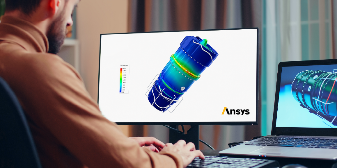
While GaN and SiC offer remarkable intrinsic advantages, realizing their full potential requires meticulous system-level optimization. This is where Ansys simulation platforms become indispensable, enabling engineers to model, simulate, and validate every nuance of thermal, electromagnetic, and power behavior before prototyping.
Key Ansys Tools in Action:
Ansys Icepak – Advanced thermal simulation for managing heat dissipation in SiC-based systems.
Ansys Twin Builder – Accelerates system-level design for EV powertrains through co-simulation of electrical and mechanical domains.
Ansys SIwave – Ensures PCB signal integrity and power stability in compact GaN circuits.
Ansys HFSS – High-frequency electromagnetic modeling tailored for GaN's role in RF and radar systems.
Real-Life Examples of SiC & GaN semiconductors
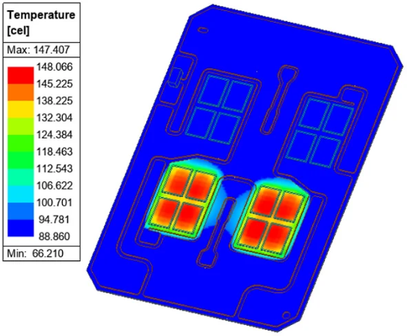
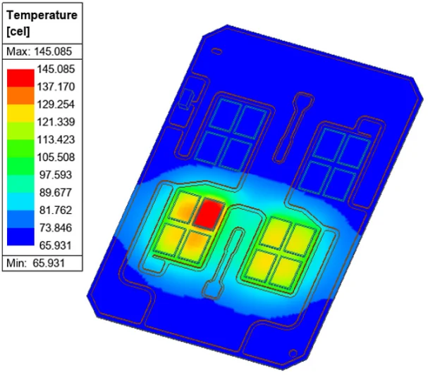
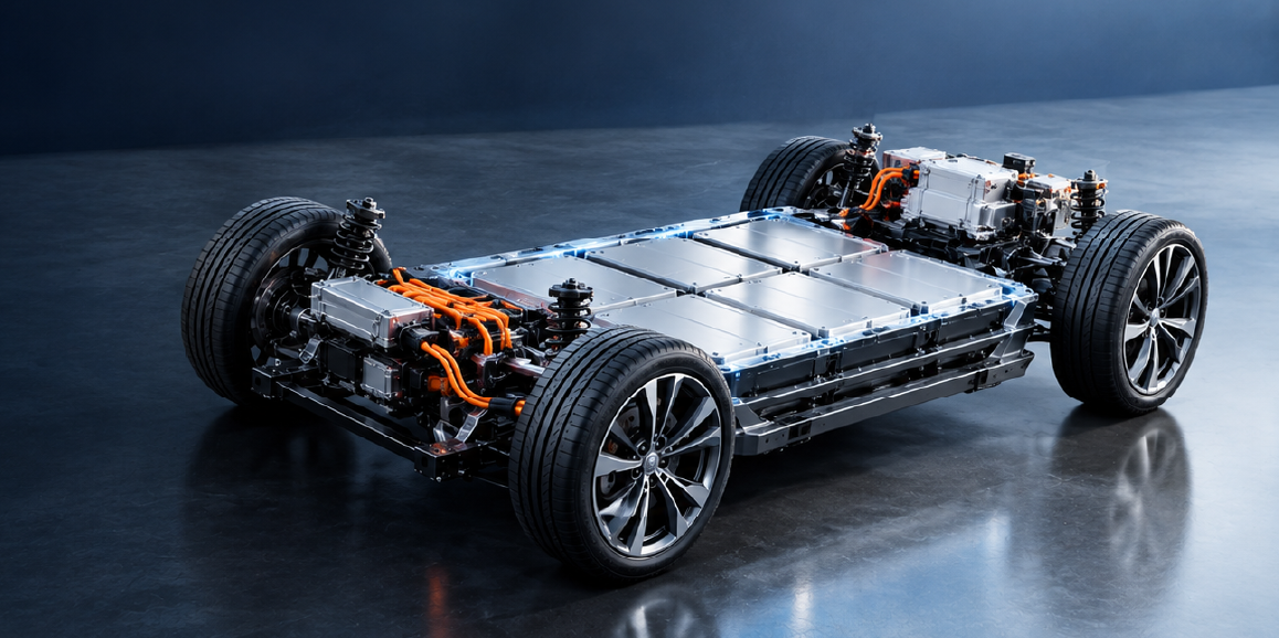
SiC Traction Inverter Optimization (EV Applications) Leveraging Ansys Icepak, engineers simulated airflow patterns and heat sink topologies in SiC-based traction inverters, reducing thermal hotspots by 20%, which directly extended device lifespan and operational stability.
GaN DC-DC Converter Design (Consumer Electronics) Using Ansys SIwave, designers predicted and minimized voltage ripple in compact GaN-based converters, enhancing EMI performance and power conversion efficiency.
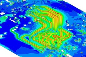
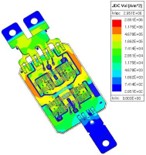
Power module thermal map, single switch temperature behavior
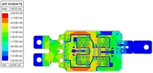
Current density map from dc+ to dc-
5. Shaping the Future: GaN and SiC in Industry Applications
Electric Vehicles
SiC MOSFETs: Enabling ultra-fast charging, longer driving ranges, and high-efficiency inverters.
GaN: Powering compact, thermally optimized onboard chargers and auxiliary systems.
Aerospace & Defense
GaN: Critical in high-frequency radar and satellite communications for real-time responsiveness.
SiC: Withstands extreme thermal conditions, ideal for deep space power systems.
Medical Technology
GaN: Provides high-frequency precision for minimally invasive surgical tools.
SiC: Supports stable power in high-performance MRI and diagnostic equipment.
6. Conclusion: From Possibility to Power
GaN and SiC semiconductors are not just the future, they are the present of power electronics innovation. As the world pivots to smarter, faster, and more energy-conscious solutions, these materials will underpin everything from zero-emission transportation to orbital communications.
Ansys simulation ecosystems enable this transformation by bridging the gap between material potential and practical design, allowing engineers to validate, optimize, and scale disruptive technologies with confidence.
Found this useful? Share it
Continue Reading
More from our engineers.
If this article was useful, these picks up where it leaves off — practical reads from the CADFEM engineering practice.