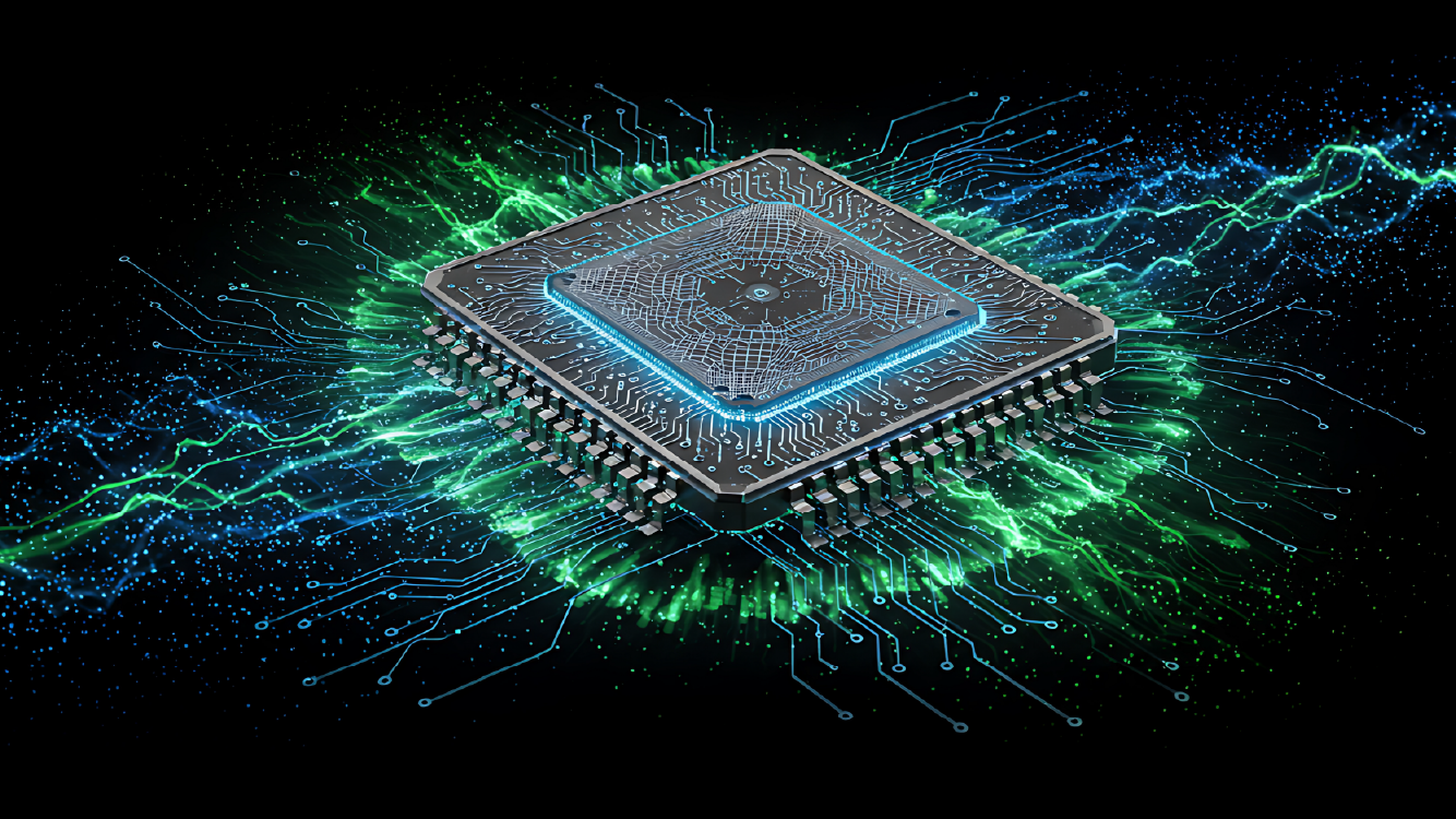
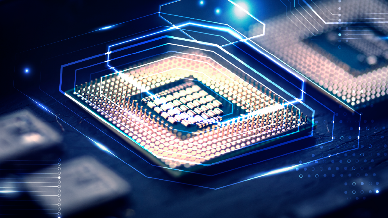
Rising Design Complexity Across Chip–Package–Board Levels
As integration scales, managing electrical, thermal, and physical interactions across multiple design layers becomes increasingly difficult.
Simulation-driven insights for signal integrity, reliability, and high-performance system integration.
Overview
The electronics and semiconductor industries are at the heart of digital transformation — powering everything from smart devices and data centers to electric vehicles and aerospace systems. With increasing product complexity, tighter power and thermal constraints, and the push for miniaturization, engineers face mounting challenges in design, validation, and reliability.
CADFEM, with Ansys solutions, empowers companies to digitally design and validate their products across the chip–package–board–system hierarchy. Whether you're optimizing signal integrity in high-speed PCBs, simulating thermal reliability in 3D ICs, or validating EMI/EMC performance, our multiphysics simulation workflows help you innovate faster, reduce failures, and comply with global standards.
As integration scales, managing electrical, thermal, and physical interactions across multiple design layers becomes increasingly difficult.
High-speed designs face EMI issues and signal integrity challenges that compromise performance and compliance.
Electronics are increasingly vulnerable to thermal stress and mechanical fatigue, impacting reliability and longevity.
Market demands push for faster design-to-silicon cycles, leaving less room for physical validation and iteration.
Designs must now adhere to multiple overlapping international standards, increasing the complexity of verification.
Space-constrained applications like consumer electronics and EVs require power-efficient, highly reliable systems.
Solution with Simulation
Solve from transistor to system with multiphysics accuracy.
Avoid re-spins by detecting risks early.
Reduce overheating, ensure packaging integrity.
Accelerate signoff timelines with validated solvers.
Improve PI/SI, thermal, and EMI performance.
Validate chiplet and 3D-IC integration.
Power Integrity & Signal Integrity
As digital systems scale toward multi-GHz signaling, multi-gigabit SerDes, DDR5/DDR6, and PCIe Gen5/6, both power integrity (PI) and signal integrity (SI) become critical bottlenecks. Noise on the power delivery network (PDN) directly couples into high-speed signals, while discontinuities in signal paths create jitter, eye closure, and data corruption. CADFEM, with Ansys solutions, provides end-to-end PI/SI workflows spanning chip-package-board-system, enabling early detection of bottlenecks, optimized decoupling, and compliance-ready channel validation.
Rapid current transients in SoCs create PDN instability, reducing timing margins.
As signaling speeds push beyond 32–112 Gbps, small discontinuities cause severe timing violations.
Incomplete return paths at vias/connectors lead to EMI leakage, SI degradation, and PDN resonance.
Balancing capacitor size, placement, and mounting inductance becomes increasingly complex in dense layouts.
TSVs, micro-bumps, and interposers introduce coupling paths not seen in traditional PCBs.
Noise coupling between PDN and signal channels must be validated together, not in isolation.
Channels must simultaneously meet compliance for multiple protocols (e.g., DDR + PCIe on the same board).
Early-stage PDN voltage-drop maps across chip-package-board.
Target impedance validation across the frequency spectrum.
Statistical and time-domain compliance checks for high-speed serial links.
Automated setup for DDR3/4/5 and LPDDR compliance tests (timing, reflections, crosstalk).
Unified modeling of die, interposer, package, and PCB for 2.5D/3D IC systems.
PDN noise injection into signal simulations for real-world correlation.
Sweeping via geometries, trace widths, stackups, and capacitor types to optimize design.
Chip-level PI/EMIR with system-level package/PCB correlation.
PCIe Gen6, 112G SerDes, DDR5/DDR6 memory interfaces.
LPDDR5/6, USB4, HDMI, high-density SoC packaging.
High-speed links in ADAS, infotainment, and ECU platforms.
Robust PDN and SI design for mission-critical electronics.
Advanced EMI/EMC & Shielding
Electronics today operate in environments saturated with electromagnetic fields — from 5G base stations and IoT hubs to aircraft, defense platforms, and mission-critical data centers. Ensuring compliance, shielding, and resilience against EMI/EMC threats is a major design and certification challenge, and physical EMC testing is expensive and iterative. CADFEM, powered by Ansys solutions, enables virtual compliance — covering Radiated Emissions (RE), Conducted Emissions (CE), ESD, immunity, shielding effectiveness, and reverberation chambers — accelerating product readiness while reducing costly lab cycles.
Meeting CISPR 11/22/32, FCC Part 15, MIL-STD-461, DO-160, ISO 11452, and IEC 61000 EMC standards.
EMC chambers, RE/CE test benches, and shielding tests are expensive with multiple re-spins common.
Long cables act as antennas, amplifying conducted/radiated emissions and susceptibility.
Balancing airflow for cooling with EMI shielding in dense electronic enclosures.
Defense, aerospace, and critical infrastructure must withstand HIRF, EMP, and lightning.
HIRF, lightning strike, RE/CE compliance, shielding of avionics and radomes.
EMC compliance of EV electronics, busbars, inverters, and harnesses (RE, CE, immunity).
Rack-level shielding, reverberation chamber-based compliance, RE control.
Shielding of power cabinets, substations, renewable inverters under CE/RE stress.
EMC validation of implants, diagnostic instruments, and life-critical equipment.
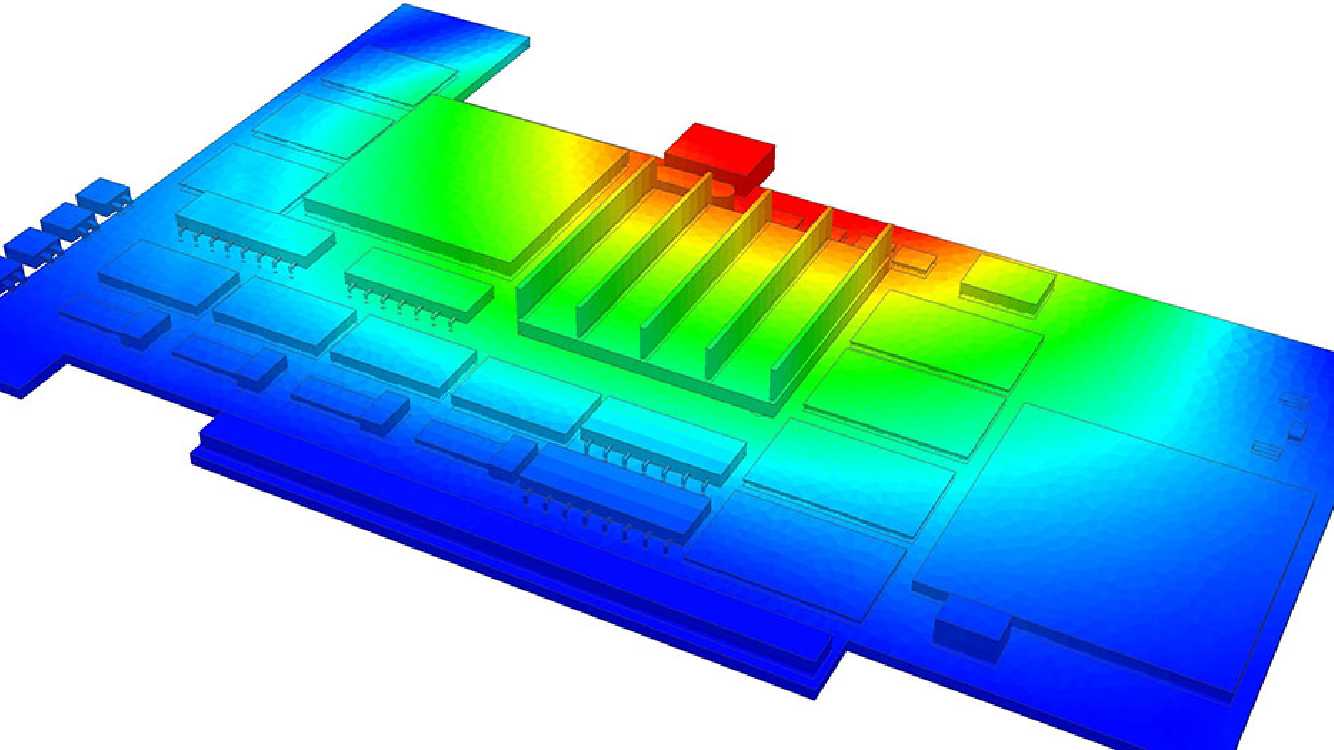
Thermal & Mechanical Reliability
From hot-spots to solder fatigue and drop events, CADFEM's multiphysics reliability workflows simulate thermal, structural, and shock/vibration stresses to predict product life before hardware build.
Power-dense chips develop thermal hotspots that reduce performance and lifetime.
Cyclic thermal loads cause solder joint degradation, especially in automotive and aerospace applications.
Layered packages are susceptible to warping due to material mismatches and thermal stress.
Mechanical deformations during transport or usage can lead to cracks and electrical failure.
Multiphysics interactions must be analyzed together to ensure real-world robustness.

Advanced Packaging & 3D IC
The semiconductor industry is rapidly transitioning to heterogeneous integration and advanced packaging to keep pace with Moore's Law alternatives. Chiplets, interposers, and 3D stacked dies offer higher bandwidth, lower latency, and improved power efficiency — but they also introduce complex multiphysics challenges spanning electrical, thermal, and mechanical domains. CADFEM, with Ansys multiphysics platforms, provides foundry-certified sign-off workflows for advanced packaging and 3D ICs, ensuring reliability from chiplet-to-system.
Electromagnetic and thermal coupling between closely stacked dies increases leakage and crosstalk risks.
Limited cooling pathways lead to hotspots, reliability degradation, and accelerated aging.
Dense TSV and RDL networks increase SI/PI challenges at 112G SerDes, DDR5/6, and HBM speeds.
CTE (Coefficient of Thermal Expansion) mismatches induce stress and delamination in 2.5D/3D stacks.
Packaging success depends on seamless integration of electrical, thermal, and structural solvers.
Complex heterogeneous integration poses yield, alignment, and assembly challenges.
Integrated flows bridging die power models (RedHawk-SC), package parasitics (Q3D), and board SI/PI (SIwave).
Chip-to-system temperature-aware power integrity analysis to prevent thermal runaway.
Predicting deformation of interposers and substrates during reflow, assembly, and operation.
Channel compliance analysis for HBM, PCIe Gen6, CXL, and custom chiplet links.
Solder fatigue, TSV reliability, and thermal cycling stress validation.
Incorporating ESD, IR drop, and EMIR validation into early package sign-off.
HBM-enabled GPUs, CPUs, and AI accelerators with stacked 3D memory.
Chiplet-based AP/Modem/Memory integration for smartphones and AR/VR devices.
Reliable 2.5D/3D ICs for ADAS, infotainment, and EV control units.
112G SerDes, optical/electrical co-packaging, and chiplet-based CXL/PCIe architectures.
Radiation-hardened 2.5D/3D ICs with strict thermal and reliability requirements.

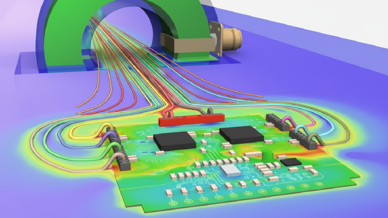
Antenna & Wireless System Integration
With the growing adoption of 5G, Wi-Fi 7, IoT, satellite communications, and automotive radar, antenna design has become central to electronics innovation. Antennas must not only deliver high performance in isolation but also coexist with complex PCB layouts, enclosures, human bodies, and surrounding systems. CADFEM, powered by Ansys solvers, enables engineers to virtually prototype, optimize, and integrate antennas in real-world environments — shortening design cycles and ensuring compliance.
Designing high-frequency antennas within limited space while meeting gain and efficiency targets.
Phased-array and MIMO systems require accurate modeling of element interactions to maintain beam patterns.
Wearable and automotive antennas face detuning, absorption, and compliance risks.
Smartphones, EVs, and IoT hubs integrate multiple radios, creating coexistence and EMI challenges.
Antennas must be tested virtually in enclosures, buildings, vehicles, or outdoor ranges to ensure reliable performance.
Massive MIMO base-stations, mmWave smartphone antennas.
Radar, GNSS, V2X, SATCOM, in-flight Wi-Fi.
Wearables, AR/VR devices, IoT hubs, smartphones.
High-gain phased arrays, satellite payload antennas, radomes.
Low-Frequency Electromagnetics
Electromechanical components form the backbone of energy conversion and motion systems across automotive, industrial, medical, and aerospace domains. From high-efficiency motors and actuators to robust busbars and inductive charging systems, engineers must balance electromagnetic performance, thermal reliability, and mechanical integrity. CADFEM, with Ansys solutions, provides a unified multiphysics environment to design, optimize, and validate these low-frequency electromagnetic devices.
Reducing copper and iron losses while maximizing torque density and system efficiency.
Excessive joule heating in busbars, coils, and windings reduces lifespan and reliability.
Accurate modeling of nonlinear BH-curves is critical for transformers and actuators.
Ensuring structural and thermal robustness of busbars and switchgear during transient overloads.
Validating motor performance under real drive cycles and controller algorithms.
Electromagnetic forces induce vibrations in motors and actuators, requiring coupled EM–structural simulations.
Traction motors, inverters, busbars, battery contactors, EV charging coils.
Actuators, robotics motors, solenoids for precision machinery.
Transformers, reactors, and high-current busbars in substations.
Electromagnetic actuators, solenoids, cryogenic motors, and magnetic bearings.

Data Center Simulation
Data centers are the backbone of the digital economy, supporting AI, cloud, IoT, and high-performance computing. With rising power densities, accelerated deployment timelines, and stringent energy-efficiency goals, operators face significant challenges in ensuring performance, uptime, and sustainability. CADFEM, powered by Ansys multiphysics solutions, provides end-to-end digital simulation workflows to optimize electrical infrastructure, cooling architectures, and EMI shielding for data centers at rack, room, and facility scale.
Next-gen AI/ML workloads push racks to 70–100 kW+, demanding advanced cooling strategies.
Innovative cooling introduces new reliability risks (leakage, condensation, pump failure).
Peak load conditions stress busbars, UPS systems, and switchgear, risking downtime.
Dense PCB and rack integration increases EMI, threatening server compliance and performance.
Operators face strict energy targets, requiring precise modeling of efficiency metrics.
AI-ready rack and cooling design, PUE optimization.
Reliability analysis of electrical distribution and redundancy.
Compact footprint cooling, EMI/EMC compliance.
Multi-tenant thermal, electrical, and shielding optimization.
Ruggedized, fault-tolerant, and EMI-hardened data center design.