Bridging the Gap: Edge Couplers in Photonic Integrated Circuits
Edge couplers facilitate efficient light transfer between optical fibers and on-chip waveguides. See how to design and optimize them for SOI platforms at 1550 nm.
AP
Akankshya Panigrahi
Apr 18, 20255 min read
Edge couplers are vital components in photonic integrated circuits (PICs), facilitating efficient light transfer between optical fibers and on-chip waveguides. The Ansys Optics article provides a comprehensive guide on designing and optimizing edge couplers, particularly for silicon-on-insulator (SOI) platforms operating at a 1550 nm wavelength.
Understanding Edge Couplers
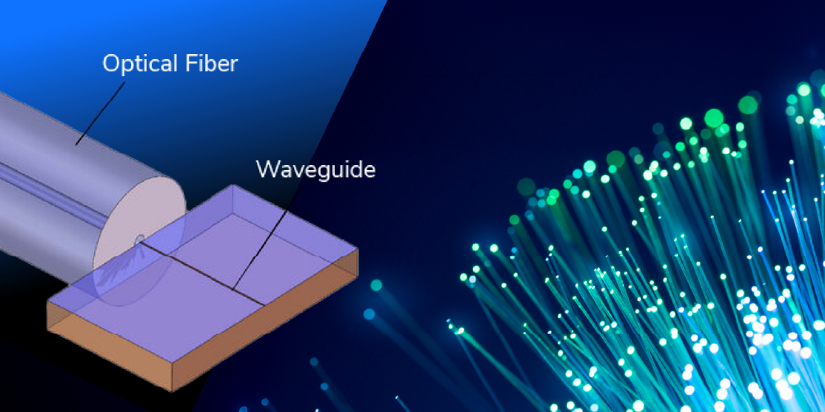
Edge couplers function by aligning an optical fiber directly to the edge of a photonic chip, allowing in-plane light coupling. This method is especially beneficial for applications requiring high coupling efficiency and broad bandwidth.
The Ansys example focuses on designing an edge coupler that efficiently couples light between a standard SMF-28 optical fiber and an integrated waveguide. Key design features include:
Multi-layer Si₃N₄ Structure: Three silicon nitride layers are employed to gradually expand the optical mode, facilitating better mode matching with the fiber.
Inverse Silicon Taper: A tapering silicon structure narrows towards the chip edge, aiding in mode size transformation and minimizing reflection losses.
Sub-wavelength Gratings: These structures effectively grade the refractive index, enhancing mode matching between the fiber and waveguide.
The design process utilizes simulation tools like the Eigenmode Expansion (EME) method to optimize parameters such as fiber position and taper length, achieving a modal overlap efficiency of approximately 93%.
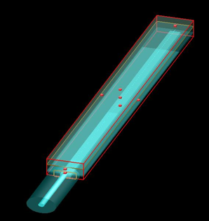
Edge coupler 3D view
Procedure for Creating an Edge Coupler
Designing an edge coupler involves a series of simulation and optimization steps to ensure efficient light transfer between a single-mode fiber and an on-chip waveguide. Here's a concise overview of the procedure based on the Ansys Optics workflow:
Mode Analysis (FDE Tool): Begin by using the Finite-Difference Eigenmode (FDE) solver to determine the optimal fiber position. This is done by maximizing the mode overlap between the fiber mode and the coupler mode at the operating wavelength (typically 1550 nm).
Initial EME Simulation: Perform an Eigenmode Expansion (EME) simulation to optimize the inverse taper's length and geometry without including the substrate. This simplifies computation and helps in understanding the coupling trend.
Substrate Inclusion: Next, reintroduce the silicon substrate into the simulation. This step is critical to account for potential leakage losses into the substrate, and adjust the taper geometry accordingly.
S-Parameter Extraction: Simulate across a wavelength sweep to extract the S-parameters (transmission and reflection data), which characterize the coupler's optical performance.
Compact Model Generation: Use the S-parameters to create a compact model in Ansys INTERCONNECT for system-level simulations.
Advanced Optimization: For enhanced accuracy, incorporate sub-wavelength gratings and use graded-index profiles. Use analysis groups to manage parameters and enable quick design updates.
This structured simulation flow ensures optimal coupling efficiency, minimal loss, and compatibility with fiber interfacing in PIC applications.
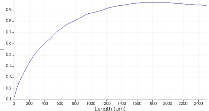
EME sweep data of taper lengthOutput mode
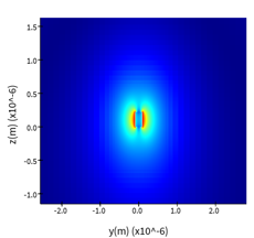
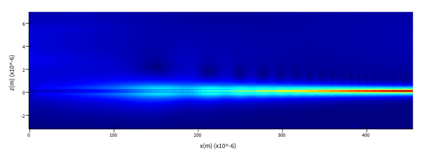
Mode profile in x-z plane
Comparing Edge Couplers with Other Coupling Methods
In PICs, several coupling techniques are employed, each with its advantages and limitations:
1. Grating Couplers
Grating couplers use diffractive structures to couple light vertically into the chip.
Advantages:
Flexible Placement: Can be positioned anywhere on the chip surface.
Wafer-Level Testing: Facilitates testing before chip dicing.
Polarization Sensitivity: Performance can vary with light polarization.
2. Evanescent Couplers
Evanescent couplers rely on the overlap of evanescent fields between adjacent waveguides.
Advantages:
High Coupling Efficiency: Often around 1.0 dB.
Broad Bandwidth: Suitable for wavelength-division multiplexing.
Good Alignment Tolerance: Less sensitive to positioning errors.
Limitations:
Complex Fabrication: Requires precise control over waveguide spacing.
Limited to Specific Designs: Not as versatile for all PIC layouts.
3. Edge Couplers
As discussed, edge couplers offer high efficiency and broad bandwidth but come with their own set of challenges.
Advantages:
High Coupling Efficiency: Approximately 1.2 dB insertion loss.
Wide Bandwidth: Up to 200 nm for TE modes.
Polarization Independence: Less sensitive to light polarization.
Limitations:
Fabrication Complexity: Requires precise cleaving and polishing of the chip edge.
Fixed Coupling Position: Limited to the chip's edge, restricting design flexibility.
Larger Footprint: Occupies more space compared to grating couplers.
Conclusion
Edge couplers are indispensable for applications demanding high coupling efficiency and broad operational bandwidth in photonic integrated circuits. While they pose fabrication and design challenges, their performance benefits often outweigh these drawbacks, especially in high-speed data communication systems. When selecting a coupling method, engineers must balance factors like efficiency, bandwidth, fabrication complexity, and design flexibility to meet specific application requirements.
Found this useful? Share it
Continue Reading
More from our engineers.
If this article was useful, these picks up where it leaves off — practical reads from the CADFEM engineering practice.